A copy of this work was available on the public web and has been preserved in the Wayback Machine. The capture dates from 2017; you can also visit the original URL.
The file type is application/pdf.
Filters
Top–Down Fabrication of Gate-All-Around Vertically Stacked Silicon Nanowire FETs With Controllable Polarity
2014
IEEE transactions on nanotechnology
Preserved Fulltext
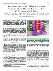
In this paper, we report on the fabrication of novel ambipolar Silicon nanowire (SiNW) Schottky-barrier (SB) FET transistors featuring two independent gate-all-around electrodes and vertically stacked ...
Measurement results on silicon show I on /I off > 10 6 and subthreshold slopes approaching the thermal limit, SS ≈ 64 mV/dec (70 mV/dec) for p(n)-type operation in the same physical device. ...
Fig. 4 . 4 SEM/FIB cross sections of fabricated devices, showing the (a) nanowire stack with 8-nm gate oxide and 50-nm thick conformal polysilicon GAA structure; and (b) optimized d < 20-nm stacked nanowires ...
doi:10.1109/tnano.2014.2363386
fatcat:ddok3ovf3fhtpnxnkcbcd2hnby
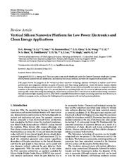
Vertical Silicon Nanowire Platform for Low Power Electronics and Clean Energy Applications
2012
Journal of Nanotechnology
Preserved Fulltext
A copy of this work was available on the public web and has been preserved in the Wayback Machine. The capture dates from 2019; you can also visit the original URL.
The file type is application/pdf.
, (2) a natural platform for tunneling FETs, and (3) a route to fabricate stacked nonvolatile memory cells. ...
This paper reviews the progress of the vertical top-down nanowire technology platform developed to explore novel device architectures and integration schemes for green electronics and clean energy applications ...
Acknowledgment The authors acknowledge the support from Semiconductor Process Technologies Lab of the Institute of Microelectronics/A * STAR, Singapore in samples preparation and analysis. ...
doi:10.1155/2012/492121
fatcat:lz6n5lw4sbg4zaemapafx3o7jq
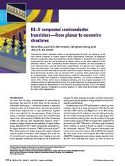
III–V compound semiconductor transistors—from planar to nanowire structures
2014
MRS bulletin
Preserved Fulltext
A copy of this work was available on the public web and has been preserved in the Wayback Machine. The capture dates from 2018; you can also visit the original URL.
The file type is application/pdf.
As discussed, optimization of the gate stack for small EOT and D it and reduction of parasitic resistances are also necessary for TFETs, similar to III-V MOSFETs. ...
This could be addressed by tunnel FETs (TFETs), which rely on interband tunneling and thus require advanced III-V heterostructures for optimized performance. ...
As discussed, optimization of the gate stack for small EOT and D it and reduction of parasitic resistances are also necessary for TFETs, similar to III-V MOSFETs. ...
doi:10.1557/mrs.2014.137
fatcat:7y7gvgqpgbdrvemnrndw3rjo3m
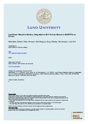
Low-Power Resistive Memory Integrated on III-V Vertical Nanowire MOSFETs on Silicon
2020
IEEE Electron Device Letters
Preserved Fulltext
A copy of this work was available on the public web and has been preserved in the Wayback Machine. The capture dates from 2020; you can also visit the original URL.
The file type is application/pdf.
III-V vertical nanowire MOSFETs (VNW-FETs) have the potential to extend Moore's law owing to their excellent material properties. ...
The combined use of VNW-FET drain metal electrode and the RRAM bottom electrode reduces the process complexity and maintains material compatibility. ...
A record high gm > 3 mS/µm and low RON = 190 Ωµm at VDS = 0.5 V have been reported on a scaled III-V VNW-FET with LG = 25 nm and a channel diameter of 17 nm with a similar process used for the selector ...
doi:10.1109/led.2020.3013674
fatcat:brrlq4ctxba4fhm6jpttclpcpq
Smooth plasma etching of GeSn nanowires for gate-all-around field effect transistors
2021
Semiconductor Science and Technology
Preserved Fulltext
A copy of this work was available on the public web and has been preserved in the Wayback Machine. The capture dates from 2022; you can also visit the original URL.
The file type is application/pdf.
We report on the nanopatterning of horizontal and vertical germanium-tin (Ge 1−x Sn x or GeSn) nanowires by inductively coupled plasma reactive ion etching for gate-all-around field effect transistors. ...
First, a chlorine based chemistry has been investigated and optimal conditions identified for GeSn 6% alloys. ...
Acknowledgments This work was partly supported by the French RENATECH network through the PTA technological platforms in Grenoble and by the EquipEx IMPACT program, managed by the ANR French agency (ANR ...
doi:10.1088/1361-6641/abfbb5
fatcat:zvzhsqhgpfdbbmi7odg6bfrzem
Sub-100nm Non-Planar 3D InGaAs MOSFETs: Fabrication and Characterization
2012
ECS Transactions
Preserved Fulltext
A copy of this work was available on the public web and has been preserved in the Wayback Machine. The capture dates from 2017; you can also visit the original URL.
The file type is application/pdf.
, and InGaAs gate-all-around nanowire MOSFETs. ...
In this paper, the fabrication and characterization of various non-planar 3D InGaAs MOSFETs have been demonstrated and summarized, including InGaAs heterostructure FinFETs, InGaAs-on-nothing nanowire MOSFETs ...
Li, and J. del Alamo for the valuable discussions and Y. Q. Liu, C. Zhang, L. Dong for technical assistance. The work is supported in part by NSF and the SRC FCRP MSD Focus Center. ...
doi:10.1149/1.3700471
fatcat:sbs7ox4gkvguxh4rpoye3vz46m
On the Vertically Stacked Gate-All-Around Nanosheet and Nanowire Transistor Scaling beyond the 5 nm Technology Node
2022
Nanomaterials
Preserved Fulltext
A copy of this work was available on the public web and has been preserved in the Wayback Machine. The capture dates from 2022; you can also visit the original URL.
The file type is application/pdf.
This work performs a detailed comparison of the channel width folding effectiveness of the FinFET, vertically stacked nanosheet transistor (VNSFET), and vertically stacked nanowire transistor (VNWFET) ...
Considering the technological constraints for the gate oxide and metal gate thicknesses, the minimum intersheet/interwire spacing should be in the range of 7 to 8 nm. ...
Comparison of (a) FinFET, (b) vertically stacked nanosheet GAA FET, and (c) vertically stacked nanowire GAA FET with the same footprint width of Wfin and fin height of Hfin. ...
doi:10.3390/nano12101739
pmid:35630961
pmcid:PMC9146649
fatcat:llnqlh75uzf7zfteuyzgh7dc4a
Materials and Devices for Nanoelectronic Systems Beyond Ultimately Scaled CMOS
[chapter]
2009
Nanosystems Design and Technology
Preserved Fulltext
A copy of this work was available on the public web and has been preserved in the Wayback Machine. The capture dates from 2017; you can also visit the original URL.
The file type is application/pdf.
Source and drain regions are highly doped (10 20 cm 3 / and 10 nm of SiO 2 is thermally grown. ...
The solution is spin-coated and baked for 5 min at 137 ı C. Two polymer layer thicknesses, of 100 and 40 nm, are studied. ...
doi:10.1007/978-1-4419-0255-9_2
fatcat:jr5pdhrezngbtl6dd3gsrbwpni
Silicon Nanowire Technologies: brief review, home-made solutions and future trends
2022
Journal of Integrated Circuits and Systems
Preserved Fulltext
A copy of this work was available on the public web and has been preserved in the Wayback Machine. The capture dates from 2022; you can also visit the original URL.
The file type is application/pdf.
Promising future developments in VLSI and More Than Moore applications such as vertically stacked nanowire geometries, graphene nanoribbon devices, and MagFETs are also presented. ...
Now, novel devices, as well as channel and device stacking for 3D VLSI applications is being studied. ...
ACKNOWLEDGEMENTS The authors would like to acknowledge the staff at INCT-Namitec, CCS-Nano, LNNano and LPD-IFGW for their support and services, and CNPq, CAPES and FAPESP for the research funding. ...
doi:10.29292/jics.v17i2.614
fatcat:cg4fpzllynhebpcrifvimbrldq
3D GaN nanoarchitecture for field-effect transistors
2019
Micro and Nano Engineering
Preserved Fulltext
A copy of this work was available on the public web and has been preserved in the Wayback Machine. The capture dates from 2020; you can also visit the original URL.
The file type is application/pdf.
In this paper, we review the current status of 3D GaN FETs and discuss their concepts, fabrication techniques, and performances. ...
For higher power application, vertical FETs based on regular arrays of GaN nanostructures are particularly promising due to their parallel integration capability and large sidewall surfaces, which can ...
The authors thank Friedhard Römer and Bernd Witzigmann from the University of Kassel, Germany for simulation of the GaN nanowire devices and constructive discussion on the topic of 3D GaN electronics. ...
doi:10.1016/j.mne.2019.04.001
fatcat:szdm7zil2vatvmgggoafmuqd34
Optimization of Structure and Electrical Characteristics for Four-Layer Vertically-Stacked Horizontal Gate-All-Around Si Nanosheets Devices
2021
Nanomaterials
Preserved Fulltext
A copy of this work was available on the public web and has been preserved in the Wayback Machine. The capture dates from 2021; you can also visit the original URL.
The file type is application/pdf.
In this paper, the optimizations of vertically-stacked horizontal gate-all-around (GAA) Si nanosheet (NS) transistors on bulk Si substrate are systemically investigated. ...
Finally, 4 stacked GAA Si NS channels with 6 nm in thickness and 30 nm in width were firstly fabricated on bulk substrate, and the performance of the stacked GAA Si NS devices achieved a larger ION/IOFF ...
Acknowledgments: Thank you to Yongliang Li and Yongkui Zhang for results discussion; Qiuxia Xu and Hailing Tu for supervision; Junfeng Li for project administration; Wenwu Wang and Tianchun Ye for funding ...
doi:10.3390/nano11030646
pmid:33808024
pmcid:PMC7998492
fatcat:5fdijjfqpje5bffmg26lpr2epm
2020 Index IEEE Journal of the Electron Devices Society Vol. 8
2020
IEEE Journal of the Electron Devices Society
Preserved Fulltext
A copy of this work was available on the public web and has been preserved in the Wayback Machine. The capture dates from 2021; you can also visit the original URL.
The file type is application/pdf.
., JEDS 2020 1111-1117 Junctionless nanowire transistors Comparison of LER Induced Mismatch in NWFET and NSFET for 5-nm CMOS. ...
Neural Network Based Design Optimization of 14-nm Node Fully-Depleted SOI FET for SoC and 3DIC Applications. ...
Resistors Low-Voltage Hf-ZnO Thin Film Transistors With Ag Nanowires Gate Electrode and Their Application in Logic Circuit. Wu, J., +, JEDS 2020 ...
doi:10.1109/jeds.2021.3055467
fatcat:yhpqbxl4nffg7mg2cwuskvuuo4
2020 Index IEEE Transactions on Electron Devices Vol. 67
2020
IEEE Transactions on Electron Devices
Preserved Fulltext
A copy of this work was available on the public web and has been preserved in the Wayback Machine. The capture dates from 2021; you can also visit the original URL.
The file type is application/pdf.
K., and Konar, A., Optimized Substrate for Improved Performance of Stacked Nanosheet Field-Effect Transistor; TED Oct. 2020 4079-4084 Jelonnek, J., see Shcherbinin, V.I., 2933-2939 Jelonnek, J., see ...
of Hot Carrier Degradation in N-Channel Gate-All-Around Nanowire FETs; TED Jan. 2020 4-10 Gupta, C., Gupta, A., Vega, R.A., Hook, T.B., and Dixit, A., Impact of Hot-Carrier Degradation on Drain-Induced ...
Pilossof, M., +, TED April 2020 1804-1807 Optimization of Stacked Nanoplate FET for 3-nm Node. ...
doi:10.1109/ted.2021.3054448
fatcat:r4ertn5jordkfjjvorvss7n6ju
High-Performance Wrap-Gated InGaAs Nanowire Field-Effect Transistors with Sputtered Dielectrics
2015
Scientific Reports
Preserved Fulltext
A copy of this work was available on the public web and has been preserved in the Wayback Machine. The capture dates from 2019; you can also visit the original URL.
The file type is application/pdf.
Although wrap-gated nanowire field-effect-transistors (NWFETs) have been explored as an ideal electronic device geometry for low-power and high-frequency applications, further performance enhancement and ...
By combining sputtering and pre-deposition chemical passivation to achieve high-quality gate dielectrics for wrap-gated NWFETs, the superior gate coupling and electrical performances have been achieved ...
In the past decade, III-V compound semiconductor nanowires (NWs) have attracted extensive amount of research and development interest due to their excellent physical properties for high-performance nanoelectronics ...
doi:10.1038/srep16871
pmid:26607169
pmcid:PMC4660349
fatcat:a2si3amuy5dhzectaz24qeerfa
State of the Art and Future Perspectives in Advanced CMOS Technology
2020
Nanomaterials
Preserved Fulltext

A copy of this work was available on the public web and has been preserved in the Wayback Machine. The capture dates from 2020; you can also visit the original URL.
The file type is application/pdf.
This article presents a review of new architectures, simulation methods, and process technology for nano-scale transistors on the approach to the end of ITRS technology. ...
Today's transistors with 3D structure and integrated advanced strain engineering differ radically from the original planar 2D ones due to the scaling down of the gate and source/drain regions according ...
In this field, the nanowire size-effects on the electrical properties were studied in reference [26] while how to enhance single device performance for the hGAAFETs with vertically stacked nanowire/nanosheet ...
doi:10.3390/nano10081555
pmid:32784801
pmcid:PMC7466708
fatcat:yssyxekom5hslivtbxbphjg6h4
« Previous
Showing results 1 — 15 out of 401 results