A copy of this work was available on the public web and has been preserved in the Wayback Machine. The capture dates from 2018; you can also visit the original URL.
The file type is application/pdf.
Filters
Low-Cost On-Chip Clock Jitter Measurement Scheme
2015
IEEE Transactions on Very Large Scale Integration (vlsi) Systems
Preserved Fulltext
In this paper, we present a low-cost, on-chip clock jitter digital measurement scheme for high performance microprocessors. It enables in situ jitter measurement during the test or debug phase. ...
part of such ROs, thus allowing to measure clock jitter with a very limited cost increase compared with PPV measurement only, and with no impact on parameter variation measurement resolution. ...
Based on the limitations of the approaches proposed so far to achieve high jitter measurement resolution and accuracy at limited costs, in this paper, we present a new on-chip digital measurement scheme ...
doi:10.1109/tvlsi.2014.2312431
fatcat:mljqvrbmjvfgnhv3lk3oddstji
On-chip jitter tolerance measurement technique with independent jitter frequency modulation from VCO in CDR
2015
IEICE Electronics Express
Preserved Fulltext
A copy of this work was available on the public web and has been preserved in the Wayback Machine. The capture dates from 2018; you can also visit the original URL.
The file type is application/pdf.
We present an on-chip measurement technique to characterize the jitter tolerance of a clock and data recovery (CDR) circuit. ...
This jitter frequency generation scheme independent from the VCO in the CDR allows a wide and linear control of jitter. ...
However, the test cost to measure the characteristics of CDR circuits on a per-chip basis is a significant portion of chip production cost. ...
doi:10.1587/elex.12.20150570
fatcat:5jqjusfkxre5vc4fbt6mkwsxy4
Jump the Q: A fast jitter tolerance measurement method using Q-statistical model
2010
2010 IEEE Electrical Design of Advanced Package & Systems Symposium
Preserved Fulltext
A copy of this work was available on the public web and has been preserved in the Wayback Machine. The capture dates from 2018; you can also visit the original URL.
The file type is application/pdf.
We present an on-chip measurement technique to characterize the jitter tolerance of a clock and data recovery (CDR) circuit. ...
This jitter frequency generation scheme independent from the VCO in the CDR allows a wide and linear control of jitter. ...
However, the test cost to measure the characteristics of CDR circuits on a per-chip basis is a significant portion of chip production cost. ...
doi:10.1109/edaps.2010.5683044
fatcat:7xlhrzgpirhndcivmdgwaplbbm
Design and Theoretical Analysis of a Clock Jitter Reduction Circuit Using Gated Phase Blending Between Self-Delayed Clock Edges
2019
IEICE Electronics Express
Preserved Fulltext

A copy of this work was available on the public web and has been preserved in the Wayback Machine. The capture dates from 2020; you can also visit the original URL.
The file type is application/pdf.
Measurement results with a 180-nm CMOS prototype chip demonstrated an approximately four-fold reduction in timing jitter from 30.2 ps to 8.8 ps in 500-MHz clock by cascading the proposed circuit with four-stages ...
By blending uncorrelated clock edges, the output clock edges approach the ideal timing and, thus, timing jitter can be reduced by a factor of per stage. ...
This paper describes the design of the low-cost, high-PVT-robust jitter reduction scheme and presents measurement results that support the claims. ...
doi:10.1587/elex.16.20190218
fatcat:32hwserghna4xezfbsxfzomxty
On-chip Jitter Measurement Using Vernier Ring Time-to-Digital Converter
2010
2010 19th IEEE Asian Test Symposium
Preserved Fulltext
A copy of this work was available on the public web and has been preserved in the Wayback Machine. The capture dates from 2017; you can also visit the original URL.
The file type is application/pdf.
This on-chip jitter measurement scheme can measure a large jitter with a fine resolution smaller than 8ps. ...
This paper presents an on-chip jitter measurement technique based on the Vernier ring time-do-digital converter (VRTDC). ...
CONCLUSION This paper presents an on-chip jitter measurement scheme using Vernier ring TDC. ...
doi:10.1109/ats.2010.38
dblp:conf/ats/YuD10
fatcat:ao55ktw6ebfsda3tfolwjgy3ay
A 960-Mb/s/pin interface for skew-tolerant bus using low jitter PLL
1997
IEEE Journal of Solid-State Circuits
Preserved Fulltext
A copy of this work was available on the public web and has been preserved in the Wayback Machine. The capture dates from 2003; you can also visit the original URL.
The file type is application/pdf.
The I/O circuit uses a low jitter phase-locked loop (PLL) which suppresses the effect of supply noise. Measured results show peakto-peak jitter of 150 ps and rms jitter of 15.7 ps on the clock line. ...
This paper describes an I/O scheme for use in a highspeed bus which eliminates setup and hold time requirements between clock and data by using an oversampling method. ...
If the phase jitter on the incoming data is low and the PLL has low jitter characteristics, the oversampling ratio can be as low as three [7] . ...
doi:10.1109/4.568836
fatcat:7rc7x2k6prdipdrqnxipraskai
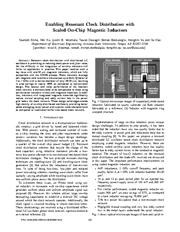
Enabling resonant clock distribution with scaled on-chip magnetic inductors
2009
2009 IEEE International Conference on Computer Design
Preserved Fulltext
A copy of this work was available on the public web and has been preserved in the Wayback Machine. The capture dates from 2017; you can also visit the original URL.
The file type is application/pdf.
Resonant clock distribution with distributed LC oscillators is promising to reducing clock power and jitter noise. ...
Yet the difficulty in the integration of on-chip inductors still limits its application in practice. ...
To extract jitter histogram, period jitter is calculated as Period Jitter = t measured − t ideal which gives the variation of the measured clock period from the ideal clock period. ...
doi:10.1109/iccd.2009.5413169
dblp:conf/iccd/SinhaXVDBYC09
fatcat:o6r3hzen6zhz5hfd5mgn7ltnei
A low-cost built-in self-test for CP-PLL based on TDC
2014
IEICE Electronics Express
Preserved Fulltext
A copy of this work was available on the public web and has been preserved in the Wayback Machine. The capture dates from 2018; you can also visit the original URL.
The file type is application/pdf.
This paper proposes a low cost BIST structure providing both the faults detected and timing jitter measured. ...
To ensure qualification of charge-pump locked-loop (CP-PLL), a complete built-in self-test (BIST) scheme should provide functions of measurement of the clock jitter and detection of faults in CP-PLL. ...
The mismatch ratio of two paths is not measured either. A referenceclock-free, high-time-resolution on-chip timing jitter measurement circuit proposed in [8] . ...
doi:10.1587/elex.11.20140247
fatcat:kfhkklchzjbjxl6bojx5eo2try
A 36 nW, 7 ppm/°C on-Chip Clock Source Platform for Near-Human-Body Temperature Applications
2016
Journal of Low Power Electronics and Applications
Preserved Fulltext
A copy of this work was available on the public web and has been preserved in the Wayback Machine. The capture dates from 2018; you can also visit the original URL.
The file type is application/pdf.
We propose a fully on-chip clock-source system in which an ultra-low-power diode-based temperature-uncompensated oscillator (OSC diode ) serves as the main clock source and frequency locks to a higher-power ...
This paper demonstrates the functionality of a locking controller that uses a periodic (counter-based) scheme implemented on-chip and a prediction (temperature-drift-based) scheme. ...
the University of Virginia, for his help with testing this chip. ...
doi:10.3390/jlpea6020007
fatcat:rmok3nqlbzelzpovdjnaz7ozci
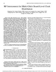
RF interconnect for multi-gbit/s board-level clock distribution
2000
IEEE Transactions on Advanced Packaging
Preserved Fulltext
A copy of this work was available on the public web and has been preserved in the Wayback Machine. The capture dates from 2017; you can also visit the original URL.
The file type is application/pdf.
In this paper, a multi-Gbit/s clock distribution scheme to minimize power consumption, skew, and jitter, based on RF interconnect technology, especially for the medium clock frequency region from 200 MHz ...
integrity problems due to clock skew, clock jitter and signal reflection. ...
(a) Demonstration of the generating on-chip digital clocks of up to 1.5 GHz using the RF clock and (b) waveforms measured at the input RF clocking signal, on-chip two-phase clock generated by the RF clock ...
doi:10.1109/6040.861553
fatcat:23cfb6xjq5hurpmr5ay5hjchae
A 2.4 Gb/s/pin simultaneous bidirectional parallel link with per-pin skew compensation
2000
IEEE Journal of Solid-State Circuits
Preserved Fulltext
A copy of this work was available on the public web and has been preserved in the Wayback Machine. The capture dates from 2003; you can also visit the original URL.
The file type is application/pdf.
This paper describes voltage and timing margins and design trade-offs in low-cost parallel links. ...
Results from a transceiver prototype demonstrate that per-pin skew compensation improves timing margins in these parallel links and can be implemented with reasonable cost overhead. ...
Mass integration of I/Os requires low cost per I/O, and the use of low-cost solutions, such as using cheaper electrical components, single-ended signalling, and simultaneous bidirectional signalling, further ...
doi:10.1109/4.881207
fatcat:o2xv4hrszrghndvmar6fgwxv5i
A generation and distribution system of clock signal source for signal acquisition system
2021
Engineering Reports
Preserved Fulltext
A copy of this work was available on the public web and has been preserved in the Wayback Machine. The capture dates from 2022; you can also visit the original URL.
The file type is application/pdf.
The system can provide the clock of low jitter which frequency is as high as 3.2 GHz. ...
The clock signal with low jitter is helpful to improve the signal-to-noise ratio (SNR) of sampled data and obtain high-precision result. ...
Hardware design of the new clock system The low jitter clock chip is the essential module in the high-speed acquisition system. ...
doi:10.1002/eng2.12494
fatcat:gwh3zxpinngmln347vat4hofly
A frequency tunable resonant clock distribution scheme using bond-wire inductor
2008
2008 Electrical Design of Advanced Packaging and Systems Symposium
Preserved Fulltext
A copy of this work was available on the public web and has been preserved in the Wayback Machine. The capture dates from 2017; you can also visit the original URL.
The file type is application/pdf.
of a conventional on-chip clock distribution. ...
In this paper, we propose a frequency control method for a resonant clock distribution scheme using a bond-wire inductor. ...
Low jitter and low skew clocking is achieved by resonator filter, and desired clock frequency is adjusted by a bond wire inductor. ...
doi:10.1109/edaps.2008.4735989
fatcat:sgwflckcm5bsfjqsww4van6bbu
8–10 Gbit/s full synthesised continuous-half-rate reference-less all-digital CDR with sub-harmonic frequency extraction
2018
Electronics Letters
Preserved Fulltext
A copy of this work was available on the public web and has been preserved in the Wayback Machine. The capture dates from 2021; you can also visit the original URL.
The file type is application/pdf.
The measured RMS jitter of the recovered clock is 2.24 ps. ...
The main purpose of CDR research is to recover clock and data from input data, preferably with a high flexibility, low-power consumption, and small chip area. ...
The measured BER reaches 10 −12 and satisfies the OC-192 jitter compliance test.Fig. 6 Recovered clock and data performance measurement result a Measured jitter performance of recovered clock b Measured ...
doi:10.1049/el.2018.6145
fatcat:adjjngr2erci5l54wiw4tsnnzu
A Fast Phase Tracking ADPLL for Video Pixel Clock Generation in 65 nm CMOS Technology
2011
IEEE Journal of Solid-State Circuits
Preserved Fulltext

A copy of this work was available on the public web and has been preserved in the Wayback Machine. The capture dates from 2017; you can also visit the original URL.
The file type is application/pdf.
Thus, it has a small chip area and low power consumption, and is well-suited to video pixel clock generation applications in 65 nm CMOS process. ...
A time-to-digital converter (TDC) and a delta-sigma modulator (DSM) are used to perform the fast phase tracking, and the tracking jitter is controlled at less than one-third of the output pixel clock period ...
The design challenges for a pixel clock generator in a digital video display system include a very high frequency multiplication ratio, a noisy low-frequency reference clock, low tracking jitter and low ...
doi:10.1109/jssc.2011.2160789
fatcat:45b7wrd7yzcjppdkaktq2zuad4
« Previous
Showing results 1 — 15 out of 4,178 results